Scanning Probe Microscopy (SPM): Microscopic Methods
Scanning probe microscopy started with scanning
tunneling microscopy (STM) in 1981 (Binnig, Rohrer; Nobel Price 1986). In
1984 the scanning near field optical microscope SNOM (or NSOM) by Pohl et al. and in 1986 the SFM
(or AFM, atomic force microscopy) by Binnig, Gerber
and Quate was added to the family of SPMs. Many more related scanning techniques have been added
since. Some of them are introduced in this document. The family of SPMs encompass scanning surface science tools that operate
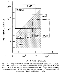
in real space with Ångstrom to nanometer spatial resolution, in contrast to
scattering techniques, such as for instance the SEM (scanning electron
microscope), that operate in the reciprocal space.
In principle, SPM systems consist of
¨ probes that are nanosized (accomplished microlithographically),
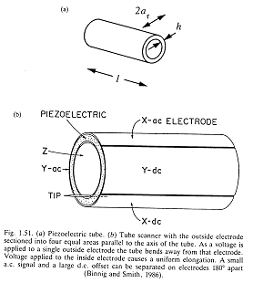
¨ scanning and feedback mechanisms that are accurate to the subnanometer level (achieved with piezoelectric material), and
¨ highly sophisticated
computer controls (obtained with fast DACs (digital analog
converters, etc.).
Probes and detection schemes involve, for instance,
etched tungsten wires and highly
sensitive preamplifiers (STM),
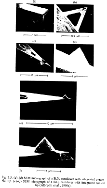
microfabricated silicon cantilevers,
low voltage laser-diodes and high
accuracy photo-diodes (SFM), and
etched optical fibers, high-powered lasers, and sensitive photodetectors
(SNOM).

Literature:
The
primarily consulted sources for the following brief instrumental review are:
-
Scanning Probe Microscopy
and Spectroscopy, Methods and Applications, R. Wiesendanger,
-
Nanoscience, Friction and Rheology on the Nanometer Scale, E. Meyer, R.M. Overney, K.
Dransfeld, T. Gyalog, World
Scientific, Singapore (1998).
SPM TREE
|
Scanning
Tunneling Microscope (STM)
|
Scanning
Force Microscope (SFM)
|
|
These are the three
basic SPM tools. |
S. Nearfield Optical Microscope (SNOM)
|


